

To meet the growing demand for advanced semiconductor technologies, semiconductor manufacturing equipment growth is expected to continue, reaching new records of $121 billion in 2025 and $139 billion in 2026, supported by both the front-end and back-end segments. Sales into the wafer fab equipment (WFE) segment are projected to expand 6.8% in 2025 and 14% in 2026, reaching $123 billion due to increased demand for advanced logic and memory applications.
Directly impacting the efficiency and yield of semiconductor manufacturing processes, wafer tables’ precision and reliability is critical in semiconductor manufacturing equipment, particularly in lithography, wafer inspection, die placement, etching and deposition machines.
3D printing can play a key role by enabling a significant change in the design architecture, not possible to produce with traditional manufacturing methods, thus driving a step change in semiconductor capital equipment accuracy, speed and uptime. It also facilitates unique wafer table designs depending on which application they address.
The Challenge
To improve wafer tables’ throughput and accuracy, and address continued miniaturization requirements, semiconductor manufacturing processes face five main challenges:
- Maintaining sub-nanometer precision over large areas
- Mitigating thermal expansion effects due to process heat
- Controlling vibrations and environmental disturbances
- Supply chain disruptions and lead times
- Traditional process limitations:
- Requires welds and/or assemblies for smooth shapes; this significantly increases production time and chance of leakage
- Walls remain relatively thick due to production limitations
- Significant compromises in function required to produce manufacturable models
- Updating designs often requires costly new tooling with long lead times
- Low production quantities often require different tooling and machines compared to high production quantities
The Solution
Enabled by our innovative metal 3D printing solutions including applications expertise, 3D Systems developed a next-generation silicon wafer table demonstrator. We implemented multiple novel design techniques to address the requirements of an ideal cooling solution.

Analysis of Cold plate solution for rapid heat dissipation
For any cold plate solution, the optimal cooling method requires:
- Rapid heat dissipation
- Uniform application of cooling medium
- Uniform surface temperature gradient
- Management of system entropy
- Heat should be directed away from the heat source as quickly as possible
Typically, cooling medium flows through snaking tubing, traversing the area where the coldest temperature state (T0) is at the entry point of the tube, and the warmest temperate state is at the exit of the tube. Design constraints typically require these two locations (entry and exit) to be collocated which adds further nonuniformity.

- Bringing the heated cooling medium back towards the T0 fluid at the entry point promotes further heat sharing to the T0 fluid lowering the overall efficiency even at the starting point.
- This design architecture is inefficient, and requires a functional compromise planar flow concept is non serial. It allows for flow across nearly the entire surface, treating it as a cavity with directional fins.
- Strong center to edge flow with waterfall edge return manifold is a novel design concept, which on its own gives a predictable polar gradient of temperature.
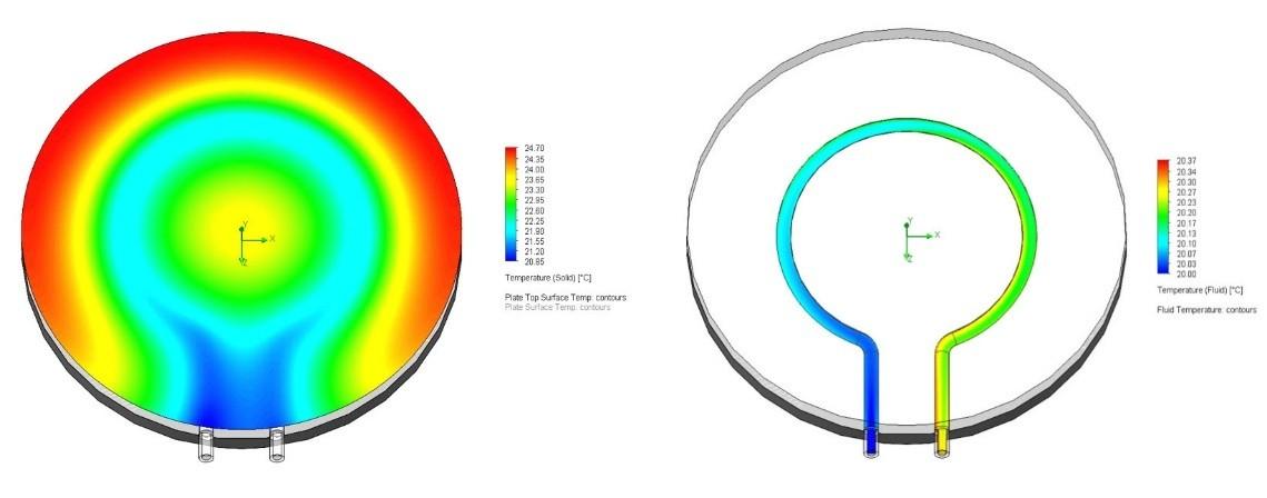
- Ideally, the cooling medium should be evenly presented across the entire cooling area, so that the lowest possible temperature is always presented to the cooling face.
In the previous point, we present a method to control the cooling profile and shape it into a polar gradient. By utilizing an industry recognized “shower head” style injector, we are evenly injecting the cooling medium into the fin array.

Analysis of showerhead solution
- This remediates the heat pickup with the previous design method of center to edge flow.
- By evenly injecting T0 fluid across the area, we damper the polar gradient and regularize the temperature across the surface while not inhibiting the flow characteristics.

- The entire contact surface should maintain the most uniform temperature
- Utilizing a generatively designed flow spreading fin network in the cooling space that we have previously shown, we provide an efficient and simple geometry to spread cooling medium in the cooling chamber.
- Combining that with the prior two design points, we have a method to manage flow and temperature gradient.
- Over time, entropy of the entire system will affect the transient total average temperature. To counteract that, there should be some methods to resist total average temperature drift
By implementing a “cold well” reservoir before the showerhead, we are allowing a volume of coolant to remain in the T0 state and provide further potential energy sink. This serves 2 purposes:- The cold well provides a continuous T0 thermal sink for the entire system, acting like an ice cube at the core, making it significantly harder for any temporal heat flux or shift to significantly affect the thermal characteristics of the system.
- Furthermore, the cold well acts as a buffer between the cooling volume and the return. It insulates the return fluid from acting on the active cooling surface with any major effect.

Analysis of metal 3D printed wafer
3D Systems offers a complete eco-system that integrates hardware, software, and services, with:
- Application Innovation Group (AIG) consulting - Together with our customers, we identify their needs, working with them to optimize designs, prototype, validate and define a manufacturing workflow.
- In this wafer table case, we used our latest advanced metal 3D printing solution: DMP Flex 350 Triple 3D printer, A6061-RAM2 alloy for high thermal conductivity, and Oqton’s 3DXpert® software.
- Technology transfer to contract manufacturer – Once validated, we help semiconductor OEMs and suppliers establish their own metal additive capabilities that reduce costs and ramp times. Our dedicated team works with you across every step, from pre-production to full-scale volume production.
Benefits / Results
Increased efficiency - Optimally design, rapidly iterate, and manufacture cold plates with complex parametric or generatively designed fluid flow pattern that accelerates fluid path evenly to increase cooling efficiency, thus improving high quality semiconductor chip yield within each wafer.
- 500x - more cooling area
- 4 -6 % - improved temperature uniformity
- 10x - increase in fluid capacity
Reliability – Single-piece cold plate prevents leakage compared to traditional cold plates comprising two or three pieces. With a monolithic design, you can express the optimal cooling medium injection, and the most efficient heat extraction.
Reduced lead-time and minimized supply chain challenges
- The lead time for a single component after development can be as low as 1 week, compared to the traditionally manufactured equivalent which would require nearly a dozen machine parts to be manufactured, as well as risky multi-piece braze welding operations, totaling at least 12 weeks.
- Added benefit and value of additive manufacturing is the ability to make design changes informed by practical testing of the first articles to further increase performance, and the ability to turn around and produce again with the same lead time.
- Production cost remains static, regardless of cooling path.
Access to metal additive manufacturing experts to develop optimized components and through expert-led technology transfer to a contract manufacturer to accelerate time-to-market.


