


As Additive Manufacturing for Semiconductor Capital Equipment race to meet growing demand for advanced chips, the pressure to improve production yield, precision, and throughput has never been greater. Industry forecasts project semiconductor manufacturing equipment spending to reach record levels in the coming years, driven by investments in advanced logic and memory applications. At the center of many fabrication processes is a critical component: the wafer table.
As chip geometries continue to shrink, even minor thermal variations or mechanical instability can reduce yield. Metal 3D printing is emerging as a powerful solution for overcoming these challenges and enabling the next generation of high-performance wafer tables.
The Challenge of Precision at the Nanoscale
Modern semiconductor manufacturing faces several significant obstacles. Wafer tables must maintain sub-nanometer precision across increasingly large surfaces while managing heat generated during processing. At the same time, manufacturers must minimize vibration, ensure system reliability, and navigate ongoing supply chain pressures.
Traditional manufacturing methods often struggle to meet these requirements. Complex cooling channels typically require multiple components, welds, and assemblies, increasing production time and creating potential leak points. Design limitations also force engineers to compromise on performance in order to create parts that can be manufactured, while design updates frequently require expensive tooling and lengthy lead times.
Rethinking Wafer Table Design with Additive Manufacturing
To address these challenges, 3D Systems developed a next-generation silicon wafer table demonstrator that leverages the design freedom of metal additive manufacturing. Rather than adapting cooling solutions to fit manufacturing constraints, engineers were able to design an optimized thermal management system specifically focused on improving temperature uniformity and heat extraction. Experts used our latest advanced metal 3D printing solution to achieve the print: DMP Flex 350 Triple 3D printer, A6061-RAM2 alloy for high thermal conductivity, and Oqton’s 3DXpert® software.
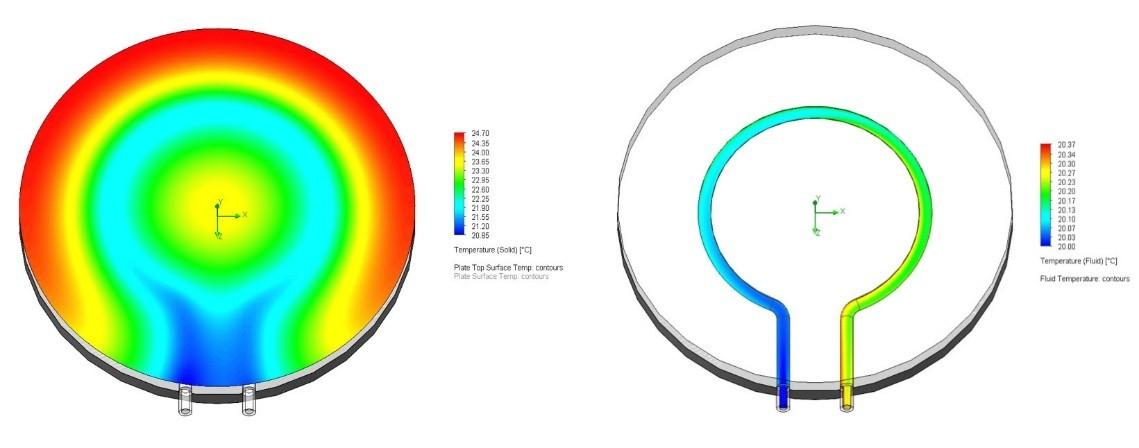
Unlike traditional cooling channels that force coolant through long, snaking tubes, the new design allows coolant to flow across nearly the entire surface area through a cavity filled with directional fins. Heated coolant exits at the perimeter, preventing warmed fluid from recirculating through the active cooling zone and improving overall heat removal efficiency.
The design also incorporates a showerhead style injector that distributes coolant uniformly across the cooling surface. By presenting the coldest available coolant evenly throughout the structure, thermal gradients are significantly reduced, helping maintain a more consistent wafer temperature during processing.
To further improve thermal performance, generatively designed fin networks optimize coolant distribution while maximizing heat transfer. A centrally located "cold well" reservoir acts as a thermal buffer, helping stabilize temperatures over time and reducing the impact of thermal fluctuations that could affect process consistency.

Direct Impact on Yield and Chip Quality
For semiconductor manufacturers, thermal stability translates directly into process quality and production yield. Wafer temperature variations can introduce dimensional inaccuracies, misalignment, and process variability that affect chip performance.
The 3D-printed wafer table demonstrated substantial improvements in cooling capability:
- 500x more cooling area
- 4% to 6% improvement in temperature uniformity
- 10x increase in fluid capacity
These gains help maintain more stable processing conditions, improving consistency across the wafer table and supporting the production of higher-quality semiconductor devices. Better temperature control also enables tighter process tolerances, which become increasingly important as feature sizes continue to shrink.
Faster Production, Greater Reliability
Beyond thermal performance, additive manufacturing provides significant operational advantages. The wafer table's monolithic construction eliminates the need for multiple assembled components and welds, dramatically reducing the risk of leaks and improving long-term reliability.
Lead times also improve significantly. After development, a completed component can be produced in as little as one week, compared to approximately 12 weeks for a traditionally manufactured assembly that may require numerous machined parts and complex brazing operations.
Perhaps most importantly, metal 3D printing allows rapid design iteration. Engineers can quickly incorporate lessons learned from testing and manufacture updated versions without tooling delays, accelerating innovation and reducing time-to-market.

Enabling the Future of Semiconductor Manufacturing
As semiconductor equipment manufacturers push toward higher throughput, tighter tolerances, and greater efficiency, additive manufacturing is proving to be much more than a production technology. By enabling radically improved wafer table designs that cannot be produced conventionally, metal 3D printing delivers better thermal management, improved reliability, faster development cycles, and ultimately higher semiconductor production yield.
Connect with our 3D Systems experts on optimizing performance without manufacturing constraints.


